


Dr. Gaurav Musalgaonkar discusses India's semiconductor journey, next-generation chip architectures, industry-academia translation, and the engineering pathways needed to turn research into scalable real-world innovation.
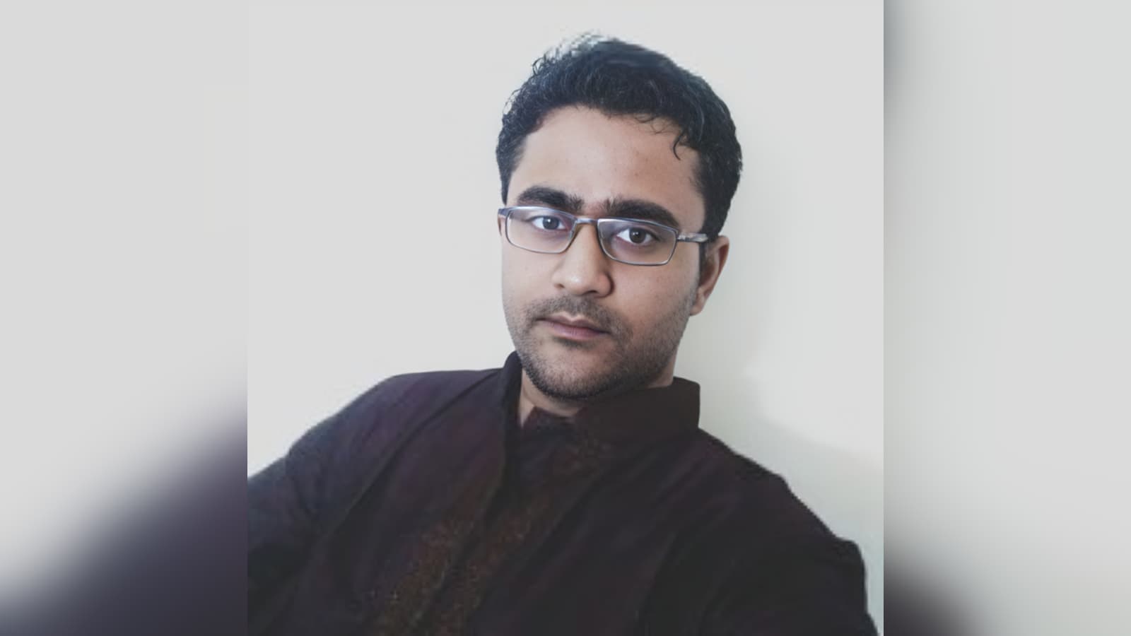
Dr. Gaurav Musalgaonkar, semiconductor researcher and device engineer, discussing advanced chip technologies and deep-tech innovation
As India accelerates its ambitions to become a global semiconductor and deep-tech powerhouse, the conversation around innovation is shifting from policy announcements to the engineering foundations that make technological self-reliance possible. In this insightful interaction with Education Post’s Prabhav Anand, Dr. Gaurav Musalgaonkar, semiconductor researcher and device engineer, explores the opportunities and challenges shaping India’s technological future. Drawing from his experience across academic research and the semiconductor industry, he discusses the evolution of next-generation transistor architectures, advances in image-sensing technologies, the growing role of AI-driven engineering, and the critical need to bridge the gap between research laboratories and real-world innovation. He also shares his perspective on India's semiconductor ambitions, deep-tech ecosystem, and the steps needed to make research careers more impactful, industry-connected, and aspirational for the next generation of engineers and innovators.
1. Through your research work, you have explored interdisciplinary and application-oriented engineering problems. What initially drew you toward this research direction, and how do you see its relevance in solving larger industrial and technological challenges in India today?

What drew me in was that semiconductor work never stays within one box. A single chip brings together physics, chemistry, materials, manufacturing, device design, and system-level application. To make real progress, you have to think across all of them.
My journey has reflected that. I started by working on silicon sensors for high-energy physics experiments, moved into CMOS/Infrared image sensors and imaging applications, and during my PhD worked on new transistor designs aimed at improving speed and power efficiency. These may look like different problems, but the common thread was always the same: taking an idea from theory or simulation and making it useful in a real technology context.
That is what kept me application-focused. I have always been most interested in work where simulations and models directly influence what can be built, whether in memory technology, advanced logic devices, or now power semiconductor products.
For India, this kind of research is especially relevant today. Semiconductors are now a national priority, and they are central to electric vehicles, renewable energy, defense, telecom, consumer electronics, and AI. Building a strong semiconductor base is not just about design or manufacturing alone; it requires connecting device physics, process technology, design, and reliability into solutions that work at scale. India already has a very strong engineering talent pool and a major role in global chip design. The next opportunity is to deepen capability across fabrication, packaging, and device technology, where hands-on, application-driven research can make a real difference.
2. A significant part of your research has focused on Tunnel FETs, nanowire architectures, and ultra-low power semiconductor devices. At a time when the global semiconductor industry is struggling with power efficiency and transistor scaling limits, how do you see these next-generation device architectures shaping the future of chip design and semiconductor innovation?
This is one of the central challenges facing the semiconductor industry. For decades, chips improved mainly by making transistors smaller. Today, the bigger limitation is power. Every transistor leaks some energy, and when billions of transistors are packed into a chip, that leakage and switching power become a major source of heat and energy consumption.
That is what drew me toward devices such as Tunnel FETs and nanowire architectures during my PhD. These devices explore ways to switch transistors using different physical mechanisms or more efficient device geometries, with the goal of reducing operating voltage and leakage. In simple terms, the aim is to do the same computation with much less energy.
I do not believe one new device will suddenly replace the conventional transistor everywhere. The semiconductor industry moves carefully because reliability, cost, and manufacturability matter as much as performance. What is more likely is that different devices will be used for the right applications: ultra-low-power devices for energy-sensitive functions, and more conventional devices where maximum performance is needed.
This is especially important in the AI era. We cannot keep solving computational demand only by building larger and hotter chips. The future will depend on getting more computation out of every unit of energy. That is why research into Tunnel FETs, nanowires, and other low-power architectures remains important, not just academically, but for the long-term sustainability of computing.
3. Your work on CMOS image sensors and HDR pixel technologies stands out because it combines device-level engineering with real-world imaging applications. What do you think are the biggest technological challenges today in improving image sensing systems, especially for applications like automotive electronics, medical imaging, and intelligent devices?
What I found most exciting about image sensors is that the physics is very direct. You are engineering how a device captures light and converts it into useful information. At the same time, the real-world requirements are becoming much more demanding.
One major challenge is dynamic range. For example, an automotive camera may have to detect objects while a car moves from a dark tunnel into bright sunlight. The sensor must capture both very dark and very bright parts of a scene without losing critical details. Achieving that inside a small pixel, without adding too much noise or cost, remains a difficult device-level challenge.
Another challenge is the trade-off between resolution and light sensitivity. Everyone wants smaller pixels and higher resolution, but smaller pixels collect less light, which can increase noise, especially in low-light conditions. A lot of device engineering goes into managing this trade-off.
For applications such as automotive electronics, medical imaging, and intelligent devices, the sensor is no longer just taking a good picture. It is providing data for decisions, sometimes safety-critical or diagnostic decisions. That means sensors must be faster, more reliable, lower power, and more intelligent. I believe the next major advances will come from combining better pixel/device design with on-sensor processing and smarter imaging architectures.
4. One aspect that makes your profile particularly interesting is the balance between academic semiconductor research and practical industry-driven innovation, including your work related to high-voltage NAND technologies and device reliability. From your experience, what is the biggest difference between how semiconductor research is approached in academia versus how it is implemented inside the industry?
I have experienced both sides, and the biggest difference is the definition of success. In academia, the focus is often on proving a new idea, a novel device concept, or a mechanism that has not been demonstrated before. There is freedom to explore deeply and ask how far a concept can be pushed in principle.
Industry asks a different question. A good idea is only the starting point. The real test is whether it can be manufactured reliably, repeatedly, and economically at scale. When I moved into NAND and DRAM memory and device reliability work, I saw very clearly that an elegant device solution is not enough if it cannot survive real processing, meet reliability targets, or support high yield.
So, academia often asks, 'Is it possible?' Industry asks, 'Is it possible, repeatable, reliable, affordable, and scalable?'
Both are essential. Academia creates bold ideas and new directions, while industry brings the discipline needed to turn those ideas into products. I believe the most impactful work happens when researchers can understand both worlds and bridge the gap between scientific novelty and practical implementation.
5. India is currently focusing heavily on building a stronger innovation and startup ecosystem. Based on your own research journey, do you think Indian institutions today are providing enough support for researchers who want to translate academic work into scalable technologies or industry-led solutions?
India has come a long way, and the intent today is much stronger than before. The talent and quality of fundamental research in Indian institutions have always been strong. What has improved recently is the national ambition around innovation, deep tech, and semiconductor development.
We are also seeing more industry investment, with semiconductor manufacturing, assembly, packaging, design, and R&D activity expanding in India. This matters because academic research needs a real destination: facilities, industry problems, and partners who can help move ideas closer to production.
The gap that still remains is translation. Moving from a promising lab result to a scalable product is difficult, especially in semiconductor technology, where the required infrastructure is expensive and the development cycle is long. A strong idea can stall if there is no clear path to prototyping, fabrication access, patient capital, or industry partnership.
So my view is that the foundation is being laid and the direction is right, but the ecosystem is still maturing. What needs to grow further is the connective tissue between academia, industry, investors, and manufacturing infrastructure. If India can strengthen those bridges, many more research ideas can move from papers into real technologies and companies.
6. In your field, computational and technology-driven approaches are becoming increasingly important across engineering and scientific research. How do you see emerging technologies like AI, simulation tools, and advanced computing changing the future of engineering research in India?
This is something I am very excited about because it is changing how engineering work is done. In semiconductor development, simulation has always been central. Before building a chip or device, we model it, test design options virtually, and eliminate weak ideas before committing time and money to fabrication. Tools like TCAD make this possible.
AI is now adding another layer of acceleration. In my own work, I have built AI-based tools to automate repetitive engineering tasks and explore large design spaces more efficiently. This allows engineers to spend less time on routine extraction and more time on deeper technical decisions.
For India, this is especially important because computation can lower the barrier to high-quality research. Not every institution can immediately access a full semiconductor fabrication facility, but many researchers can use simulation, AI, and advanced computing to develop strong ideas, optimize devices, and build valuable capability.
At the same time, computation cannot replace hardware completely. Fabs, labs, measurements, and hands-on process knowledge are still essential. The real opportunity is to combine India's software strength and engineering talent with better access to simulation tools, computing infrastructure, and industry-relevant training. That combination can make engineering research faster, more practical, and more globally competitive.
7. Looking at your own work and the broader research ecosystem, what are some areas where you believe India has strong potential to emerge as a global leader in deep-tech and applied engineering research over the next decade?
I would answer this from where I sit, having worked across both Indian academic research and the U.S. semiconductor industry. I believe India's strongest opportunities are in areas where deep engineering meets large real-world needs.
Space and defense are clear examples. India has already shown that it can deliver complex engineering outcomes with remarkable cost efficiency, and the growth of private space companies can make this sector even stronger.
Semiconductors are another major area. India already has strong design talent, and the current national focus on semiconductor manufacturing, packaging, and design is an important step. Manufacturing will take time to mature, but India can become highly competitive in chip design, AI-driven design automation, packaging, and application-specific semiconductor solutions.
Clean energy and storage are also promising because India's energy needs are massive, and the country has strong motivation to develop scalable and affordable solutions.
Overall, I see India's biggest deep-tech opportunity in combining software strength, engineering talent, and large domestic demand. The next decade will depend on how well India connects talent, capital, industry partnerships, and long-term patience into finished technologies.
8. Young researchers today often feel that core scientific and engineering research is intellectually rewarding but professionally uncertain. Based on your own academic and research experience, what changes are needed to make research careers more impactful, industry-connected, and aspirational for students in India?
This is a real concern, and I felt some of it myself. Core research is intellectually rewarding, but young researchers are not wrong to worry about career uncertainty. The work is long, the outcome is not always predictable, and students can sometimes feel they are falling behind peers who choose more direct industry paths.
The biggest change needed is a stronger connection between research and industry. Students are more motivated when they can see a clear line from the lab to a real product, company, or societal problem. This means more industry collaborations, more PhD internships inside companies, more joint projects, and more faculty-industry interaction.
The second change is financial stability. Research careers should be made more viable through better fellowships, competitive stipends, clearer career tracks, and stronger support during the most demanding years of training.
The third is better support for translation. Many good research ideas never move beyond publication because researchers lack access to prototyping, patent commercialization support, startup funding, or patient capital. Stronger mechanisms for spin-offs and deep-tech startups would make research feel like a launchpad rather than a dead end.
Finally, research needs more visibility and respect in the public imagination. We celebrate entrepreneurs and engineers, but we should also celebrate scientists and researchers who build deep technologies. When students see such people as role models, research becomes not a sacrifice, but an ambitious and impactful career choice.

Connecting Talent and Industry Will Define India’s Next Decade

UGC seeks governors’ intervention as 82 Tamil Nadu institutions face 150 fee-refund complaints

Engineering Must Build Foundations, Not Chase Every Trend: Dr. Arya Kumar Bhattacharya

Beyond Machine Intelligence: A Sanatan view of Singularity

Seven days to reopen Hormuz? Iran puts the ball in Trump's court as US standoff deepens
UGC seeks governors’ intervention as 82 Tamil Nadu institutions face 150 fee-refund complaints
Engineering Must Build Foundations, Not Chase Every Trend: Dr. Arya Kumar Bhattacharya

France protests escalate as Macron rejects minister’s resignation, students block Louvre

France protests turn violent as Paris reports 855 arrests, fresh clashes erupt

A whale’s death inspired him at four, now 11-year-old is set for Earth Medal
Connecting Talent and Industry Will Define India’s Next Decade
UGC seeks governors’ intervention as 82 Tamil Nadu institutions face 150 fee-refund complaints
Engineering Must Build Foundations, Not Chase Every Trend: Dr. Arya Kumar Bhattacharya
Beyond Machine Intelligence: A Sanatan view of Singularity
Seven days to reopen Hormuz? Iran puts the ball in Trump's court as US standoff deepens
UGC seeks governors’ intervention as 82 Tamil Nadu institutions face 150 fee-refund complaints
Engineering Must Build Foundations, Not Chase Every Trend: Dr. Arya Kumar Bhattacharya
France protests escalate as Macron rejects minister’s resignation, students block Louvre
France protests turn violent as Paris reports 855 arrests, fresh clashes erupt
A whale’s death inspired him at four, now 11-year-old is set for Earth Medal
Copyright© educationpost.in 2026 All Rights Reserved.